- USD
- CNY
- HKD
- EUR
- العربية
- čeština
- dansk
- Deutsch
- Ελληνικά
- English
- Español
- Français
- ic
- Italiano
- Netherlands
- norsk Språk
- język polski
- pt
- Português
- 中文
Texas Instruments Price List
Model | Description | Leading | Price |
---|---|---|---|
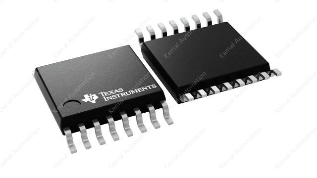
12-Bit, 82SPS, 8-Ch Delta-Sigma ADC with Temp Sensor, INT / EXT Voltage Reference & I2C Interface The ADC128D818 I2C system monitor is designed for maximum flexibility. The system monitor can be configured for single-ended and/or pseudo-differential inputs. An onboard temperature sensor, combined with WATCHDOG window comparators, and an interrupt output pin, INT, allow easy monitoring and out-of-range alarms for every channel. A high performance internal reference is also available to provide for a complete solution in the most difficult operating conditions. The ADC128D818’s 12-bit delta-sigma ADC supports Standard Mode (Sm, 100 kbps) and Fast Mode (Fm, 400 kbps) I2C interfaces. The ADC128D818 includes a sequencer to control channel conversions and stores all converted results in independent registers for easy microprocessor retrieval. Unused channels can be shut down independently to conserve power. The ADC can use either an internal 2.56-V reference or a variable external reference. An analog filter is included on the I2C digital control lines to provide improved noise immunity. The device also includes a TIME-OUT reset function on SDA and SCL to prevent I2C bus lock-up. The ADC128D818 operates from 3-V to 5.5-V power supply voltage range, –40°C to 125°C temperature range, and the device is available in a 16-pin TSSOP package. |
In Stock
|
Subscribe
|
|
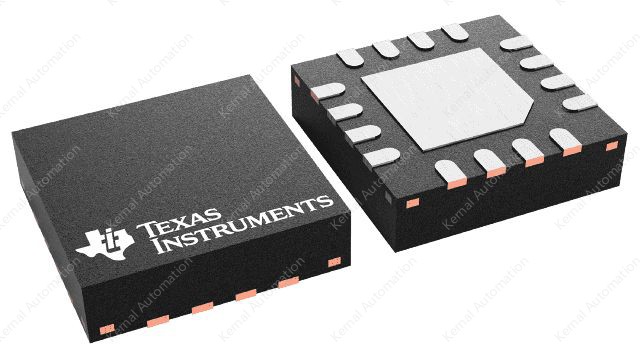
24-bit, 2-kSPS, 4-ch, low-power, small-size delta-sigma ADC w/ PGA, VREF, 2x IDACs & SPI interfaceData converters The ADS1220 is a precision, 24-bit, analog-to-digital converter (ADC) that offers many integrated features to reduce system cost and component count in applications measuring small sensor signals. The device features two differential or four single-ended inputs through a flexible input multiplexer (MUX), a low-noise, programmable gain amplifier (PGA), two programmable excitation current sources, a voltage reference, an oscillator, a low-side switch, and a precision temperature sensor. The device can perform conversions at data rates up to 2000 samples-per-second (SPS) with single-cycle settling. At 20 SPS, the digital filter offers simultaneous 50-Hz and 60-Hz rejection for noisy industrial applications. The internal PGA offers gains up to 128 V/V. This PGA makes the ADS1220 ideally-suited for applications measuring small sensor signals, such as resistance temperature detectors (RTDs), thermocouples, thermistors, and resistive bridge sensors. The device supports measurements of pseudo- or fully-differential signals when using the PGA. Alternatively, the device can be configured to bypass the internal PGA while still providing high input impedance and gains up to 4 V/V, allowing for single-ended measurements. Power consumption is as low as 120 µA when operating in duty-cycle mode with the PGA disabled. The ADS1220 is offered in a leadless VQFN-16 or a TSSOP-16 package and is specified over a temperature range of –40°C to +125°C. |
In Stock
|
Subscribe
|
|
The ADS7924 is a four-channel, 12-bit, analog-to-digital converter (ADC) with anI2C™ interface. Withits low-power ADC core, support for low-supply operation, and a flexible measurement sequencer thatessentially eliminates power consumption between conversions, the ADS7924 forms a completemonitoring system for power-critical applications such as battery-powered equipment and energyharvesting systems. The ADS7924 features dedicated data registers and onboard programmable digital thresholdcomparators for each input. Alarm conditions can be programmed that generate an interrupt. Thecombination of data buffering, programmable threshold comparisons, and alarm interrupts minimizethe host microcontroller time needed to supervise the ADS7924. The four-channel input multiplexer (MUX) is routed through external pins to allow acommon signal conditioning circuit to be used between the MUX and ADC, thereby reducing overallcomponent count. The low-power ADC uses the analog supply as its reference and can acquire andconvert signals in only 10 µs. An onboard oscillator eliminates the need to supply a masterclock. The ADS7924 is offered in a small 3-mm × 3-mm WQFN and is fully specified for operationover the industrial temperature range of –40°C to 85°C. 12-Bit 4-Ch MUX-Input SAR ADC With Intelligent System Power Control |
In Stock
|
Subscribe
|
|
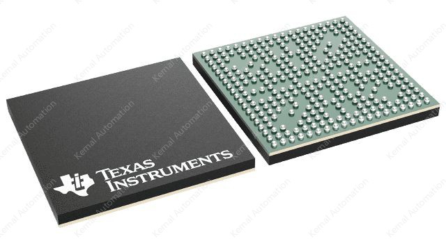
The AM335x microprocessors, based on the ARM Cortex-A8 processor, are enhanced with image, graphics processing, peripherals and industrial interface options such as EtherCAT and PROFIBUS. The devices support high-level operating systems (HLOS). Processor SDK Linux® and TI-RTOS are available free of charge from TI. The AM335x microprocessor contains the subsystems shown in the Functional Block Diagram and a brief description of each follows: The contains the subsystems shown in the Functional Block Diagram and a brief description of each follows:The microprocessor unit (MPU) subsystem is based on the ARM Cortex-A8 processor and the PowerVR SGX™ Graphics Accelerator subsystem provides 3D graphics acceleration to support display and gaming effects. The PRU-ICSS is separate from the ARM core, allowing independent operation and clocking for greater efficiency and flexibility. The PRU-ICSS enables additional peripheral interfaces and real-time protocols such as EtherCAT, PROFINET, EtherNet/IP, PROFIBUS, Ethernet Powerlink, Sercos, and others. Additionally, the programmable nature of the PRU-ICSS, along with its access to pins, events and all system-on-chip (SoC) resources, provides flexibility in implementing fast, real-time responses, specialized data handling operations, custom peripheral interfaces, and in offloading tasks from the other processor cores of SoC.。 Sitara processor: Arm Cortex-A8, 1Gb Ethernet,display,Frequency: 300 MHz |
In Stock
|
Subscribe
|
|
The AM335x microprocessors, based on the ARM Cortex-A8 processor, are enhanced with image, graphics processing, peripherals and industrial interface options such as EtherCAT and PROFIBUS. The devices support high-level operating systems (HLOS). Processor SDK Linux® and TI-RTOS are available free of charge from TI. The AM335x microprocessor contains the subsystems shown in the Functional Block Diagram and a brief description of each follows: The contains the subsystems shown in the Functional Block Diagram and a brief description of each follows:The microprocessor unit (MPU) subsystem is based on the ARM Cortex-A8 processor and the PowerVR SGX™ Graphics Accelerator subsystem provides 3D graphics acceleration to support display and gaming effects. The PRU-ICSS is separate from the ARM core, allowing independent operation and clocking for greater efficiency and flexibility. The PRU-ICSS enables additional peripheral interfaces and real-time protocols such as EtherCAT, PROFINET, EtherNet/IP, PROFIBUS, Ethernet Powerlink, Sercos, and others. Additionally, the programmable nature of the PRU-ICSS, along with its access to pins, events and all system-on-chip (SoC) resources, provides flexibility in implementing fast, real-time responses, specialized data handling operations, custom peripheral interfaces, and in offloading tasks from the other processor cores of SoC. Sitara processor: Arm Cortex-A8, 1Gb Ethernet, display, CAN,Frequency: 300 MHz |
In Stock
|
Subscribe
|
|
(The AM335x microprocessors, based on the ARM Cortex-A8 processor, are enhanced with image, graphics processing, peripherals and industrial interface options such as EtherCAT and PROFIBUS. The devices support high-level operating systems (HLOS). Processor SDK Linux® and TI-RTOS are available free of charge from TI. The AM335x microprocessor contains the subsystems shown in the Functional Block Diagram and a brief description of each follows: The contains the subsystems shown in the Functional Block Diagram and a brief description of each follows:The microprocessor unit (MPU) subsystem is based on the ARM Cortex-A8 processor and the PowerVR SGX™ Graphics Accelerator subsystem provides 3D graphics acceleration to support display and gaming effects. The PRU-ICSS is separate from the ARM core, allowing independent operation and clocking for greater efficiency and flexibility. The PRU-ICSS enables additional peripheral interfaces and real-time protocols such as EtherCAT, PROFINET, EtherNet/IP, PROFIBUS, Ethernet Powerlink, Sercos, and others. Additionally, the programmable nature of the PRU-ICSS, along with its access to pins, events and all system-on-chip (SoC) resources, provides flexibility in implementing fast, real-time responses, specialized data handling operations, custom peripheral interfaces, and in offloading tasks from the other processor cores of SoC. Sitara processor: Arm Cortex-A8, 1Gb Ethernet, display, CAN,Frequency: 600 MHz AM3352 |
In Stock
|
Subscribe
|
|
The AM335x microprocessors, based on the ARM Cortex-A8 processor, are enhanced with image, graphics processing, peripherals and industrial interface options such as EtherCAT and PROFIBUS. The devices support high-level operating systems (HLOS). Processor SDK Linux® and TI-RTOS are available free of charge from TI. The AM335x microprocessor contains the subsystems shown in the Functional Block Diagram and a brief description of each follows: The contains the subsystems shown in the Functional Block Diagram and a brief description of each follows:The microprocessor unit (MPU) subsystem is based on the ARM Cortex-A8 processor and the PowerVR SGX™ Graphics Accelerator subsystem provides 3D graphics acceleration to support display and gaming effects. The PRU-ICSS is separate from the ARM core, allowing independent operation and clocking for greater efficiency and flexibility. The PRU-ICSS enables additional peripheral interfaces and real-time protocols such as EtherCAT, PROFINET, EtherNet/IP, PROFIBUS, Ethernet Powerlink, Sercos, and others. Additionally, the programmable nature of the PRU-ICSS, along with its access to pins, events and all system-on-chip (SoC) resources, provides flexibility in implementing fast, real-time responses, specialized data handling operations, custom peripheral interfaces, and in offloading tasks from the other processor cores of SoC. Sitara processor: Arm Cortex-A8, 1Gb Ethernet, display, CAN,Frequency: 600 MHz,Operating temperature range (°C):-40 to 125 |
In Stock
|
Subscribe
|
|
The AM335x microprocessors, based on the ARM Cortex-A8 processor, are enhanced with image, graphics processing, peripherals and industrial interface options such as EtherCAT and PROFIBUS. The devices support high-level operating systems (HLOS). Processor SDK Linux® and TI-RTOS are available free of charge from TI. The AM335x microprocessor contains the subsystems shown in the Functional Block Diagram and a brief description of each follows: The contains the subsystems shown in the Functional Block Diagram and a brief description of each follows:The microprocessor unit (MPU) subsystem is based on the ARM Cortex-A8 processor and the PowerVR SGX™ Graphics Accelerator subsystem provides 3D graphics acceleration to support display and gaming effects. The PRU-ICSS is separate from the ARM core, allowing independent operation and clocking for greater efficiency and flexibility. The PRU-ICSS enables additional peripheral interfaces and real-time protocols such as EtherCAT, PROFINET, EtherNet/IP, PROFIBUS, Ethernet Powerlink, Sercos, and others. Additionally, the programmable nature of the PRU-ICSS, along with its access to pins, events and all system-on-chip (SoC) resources, provides flexibility in implementing fast, real-time responses, specialized data handling operations, custom peripheral interfaces, and in offloading tasks from the other processor cores of SoC. Sitara processor: Arm Cortex-A8, 1Gb Ethernet, display, CAN,Frequency: 300 MHz |
In Stock
|
Subscribe
|
|
The AM335x microprocessors, based on the ARM Cortex-A8 processor, are enhanced with image, graphics processing, peripherals and industrial interface options such as EtherCAT and PROFIBUS. The devices support high-level operating systems (HLOS). Processor SDK Linux® and TI-RTOS are available free of charge from TI. The AM335x microprocessor contains the subsystems shown in the Functional Block Diagram and a brief description of each follows: The contains the subsystems shown in the Functional Block Diagram and a brief description of each follows:The microprocessor unit (MPU) subsystem is based on the ARM Cortex-A8 processor and the PowerVR SGX™ Graphics Accelerator subsystem provides 3D graphics acceleration to support display and gaming effects. The PRU-ICSS is separate from the ARM core, allowing independent operation and clocking for greater efficiency and flexibility. The PRU-ICSS enables additional peripheral interfaces and real-time protocols such as EtherCAT, PROFINET, EtherNet/IP, PROFIBUS, Ethernet Powerlink, Sercos, and others. Additionally, the programmable nature of the PRU-ICSS, along with its access to pins, events and all system-on-chip (SoC) resources, provides flexibility in implementing fast, real-time responses, specialized data handling operations, custom peripheral interfaces, and in offloading tasks from the other processor cores of SoC. Sitara processor: Arm Cortex-A8, PRU-ICSS, CAN,Frequency: 600 MHz |
In Stock
|
Subscribe
|
|
The AM335x microprocessors, based on the ARM Cortex-A8 processor, are enhanced with image, graphics processing, peripherals and industrial interface options such as EtherCAT and PROFIBUS. The devices support high-level operating systems (HLOS). Processor SDK Linux® and TI-RTOS are available free of charge from TI. The AM335x microprocessor contains the subsystems shown in the Functional Block Diagram and a brief description of each follows: The contains the subsystems shown in the Functional Block Diagram and a brief description of each follows:The microprocessor unit (MPU) subsystem is based on the ARM Cortex-A8 processor and the PowerVR SGX™ Graphics Accelerator subsystem provides 3D graphics acceleration to support display and gaming effects. The PRU-ICSS is separate from the ARM core, allowing independent operation and clocking for greater efficiency and flexibility. The PRU-ICSS enables additional peripheral interfaces and real-time protocols such as EtherCAT, PROFINET, EtherNet/IP, PROFIBUS, Ethernet Powerlink, Sercos, and others. Additionally, the programmable nature of the PRU-ICSS, along with its access to pins, events and all system-on-chip (SoC) resources, provides flexibility in implementing fast, real-time responses, specialized data handling operations, custom peripheral interfaces, and in offloading tasks from the other processor cores of SoC. Sitara processor: Arm Cortex-A8, PRU-ICSS, CAN,Frequency: 800 MHz |
In Stock
|
Subscribe
|
|
The AM335x microprocessors, based on the ARM Cortex-A8 processor, are enhanced with image, graphics processing, peripherals and industrial interface options such as EtherCAT and PROFIBUS. The devices support high-level operating systems (HLOS). Processor SDK Linux® and TI-RTOS are available free of charge from TI. The AM335x microprocessor contains the subsystems shown in the Functional Block Diagram and a brief description of each follows: The contains the subsystems shown in the Functional Block Diagram and a brief description of each follows:The microprocessor unit (MPU) subsystem is based on the ARM Cortex-A8 processor and the PowerVR SGX™ Graphics Accelerator subsystem provides 3D graphics acceleration to support display and gaming effects. The PRU-ICSS is separate from the ARM core, allowing independent operation and clocking for greater efficiency and flexibility. The PRU-ICSS enables additional peripheral interfaces and real-time protocols such as EtherCAT, PROFINET, EtherNet/IP, PROFIBUS, Ethernet Powerlink, Sercos, and others. Additionally, the programmable nature of the PRU-ICSS, along with its access to pins, events and all system-on-chip (SoC) resources, provides flexibility in implementing fast, real-time responses, specialized data handling operations, custom peripheral interfaces, and in offloading tasks from the other processor cores of SoC. Sitara processor: Arm Cortex-A8, 3D graphics, PRU-ICSS, CAN,Frequency: 800 MHz |
In Stock
|
Subscribe
|
|
Sitara processor: Arm Cortex-A8, video front end (AM3517/05 is a high-performance ARM Cortex-A8 microprocessor with speeds up to 600 MHz. The device offers 3D graphics acceleration while also supporting numerous peripherals, including DDR2, CAN, EMAC, and USB OTG PHY that are well suited for industrial apllications. The processor can support other applications, including: Single-board computers Home and industrial automation Human machine Interface The device supports high-level operating systems (OSs), such as: Linux® Windows® CE Android™ The following subsystems are part of the device: Microprocessor unit (MPU) subsystem based on the ARM Cortex-A8 microprocessor PowerVR SGX graphics accelerator (AM3517 device only) subsystem for 3D graphics acceleration to support display and gaming effects Display subsystem with several features for multiple concurrent image manipulation, and a programmable interface supporting a wide variety of displays. The display subsystem also supports NTSC/PAL video out. High-performance interconnects provide high-bandwidth data transfers for multiple initiators to the internal and external memory controllers and to on-chip peripherals. The device also offers a comprehensive clock-management scheme. AM3517/05 devices are available in a 491-pin BGA package and a 484-pin PBGA package. This AM3517/05 data manual presents the electrical and mechanical specifications for the AM3517/05 Sitara processor.) |
In Stock
|
Subscribe
|
|
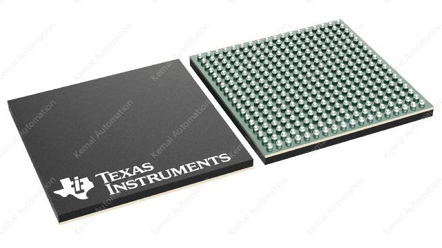
The TI AM437x high-performance processors are based on the ARM Cortex-A9 core. The processors are enhanced with 3D graphics acceleration for rich graphical user interfaces, as well as a coprocessor for deterministic, real-time processing including industrial communication protocols, such as EtherCAT, PROFIBUS, EnDat, and others. The devices support high-level operating systems (HLOS). Linux® is available free of charge from TI. Other HLOSs are available from TI’s Design Network and ecosystem partners. These devices offer an upgrade to systems based on lower performance ARM cores and provide updated peripherals, including memory options such as QSPI-NOR and LPDDR2. The processors contain the subsystems shown in the Functional Block Diagram, and a brief description of each follows. The processor subsystem is based on the ARM Cortex-A9 core, and the PowerVR SGX™ graphics accelerator subsystem provides 3D graphics acceleration to support display and advanced user interfaces. The programmable real-time unit subsystem and industrial communication subsystem (PRU-ICSS) is separate from the ARM core and allows independent operation and clocking for greater efficiency and flexibility. The PRU-ICSS enables additional peripheral interfaces and real-time protocols such as EtherCAT, PROFINET, EtherNet/IP, PROFIBUS, Ethernet Powerlink, Sercos, EnDat, and others. The PRU-ICSS enables EnDat and another industrial communication protocol in parallel. Additionally, the programmable nature of the PRU-ICSS, along with their access to pins, events and all system-on-chip (SoC) resources, provides flexibility in implementing fast real-time responses, specialized data handling operations, custom peripheral interfaces, and in off-loading tasks from the other processor cores of the SoC. High-performance interconnects provide high-bandwidth data transfers for multiple initiators to the internal and external memory controllers and to on-chip peripherals. The device also offers a comprehensive clock-management scheme. One on-chip analog to digital converter (ADC0) can couple with the display subsystem to provide an integrated touch-screen solution. The other ADC (ADC1) can combine with the pulse width module to create a closed-loop motor control solution. The RTC provides a clock reference on a separate power domain. The clock reference enables a battery-backed clock reference. The camera interface offers configuration for a single- or dual-camera parallel port. Cryptographic acceleration is available in all devices. All other supported security features, including support for Secure boot, debug security and support for Trusted execution environment is available on HS (High-Security) devices. For more information about HS devices, contact your TI sales representative. Sitara processor: Arm Cortex-A9, PRU-ICSS,Frequency: 1000 MHz |
In Stock
|
Subscribe
|
|
The TI AM437x high-performance processors are based on the ARM Cortex-A9 core. The processors are enhanced with 3D graphics acceleration for rich graphical user interfaces, as well as a coprocessor for deterministic, real-time processing including industrial communication protocols, such as EtherCAT, PROFIBUS, EnDat, and others. The devices support high-level operating systems (HLOS). Linux® is available free of charge from TI. Other HLOSs are available from TI’s Design Network and ecosystem partners. These devices offer an upgrade to systems based on lower performance ARM cores and provide updated peripherals, including memory options such as QSPI-NOR and LPDDR2. The processors contain the subsystems shown in the Functional Block Diagram, and a brief description of each follows. The processor subsystem is based on the ARM Cortex-A9 core, and the PowerVR SGX™ graphics accelerator subsystem provides 3D graphics acceleration to support display and advanced user interfaces. The programmable real-time unit subsystem and industrial communication subsystem (PRU-ICSS) is separate from the ARM core and allows independent operation and clocking for greater efficiency and flexibility. The PRU-ICSS enables additional peripheral interfaces and real-time protocols such as EtherCAT, PROFINET, EtherNet/IP, PROFIBUS, Ethernet Powerlink, Sercos, EnDat, and others. The PRU-ICSS enables EnDat and another industrial communication protocol in parallel. Additionally, the programmable nature of the PRU-ICSS, along with their access to pins, events and all system-on-chip (SoC) resources, provides flexibility in implementing fast real-time responses, specialized data handling operations, custom peripheral interfaces, and in off-loading tasks from the other processor cores of the SoC. High-performance interconnects provide high-bandwidth data transfers for multiple initiators to the internal and external memory controllers and to on-chip peripherals. The device also offers a comprehensive clock-management scheme. One on-chip analog to digital converter (ADC0) can couple with the display subsystem to provide an integrated touch-screen solution. The other ADC (ADC1) can combine with the pulse width module to create a closed-loop motor control solution. The RTC provides a clock reference on a separate power domain. The clock reference enables a battery-backed clock reference. The camera interface offers configuration for a single- or dual-camera parallel port. Cryptographic acceleration is available in all devices. All other supported security features, including support for Secure boot, debug security and support for Trusted execution environment is available on HS (High-Security) devices. For more information about HS devices, contact your TI sales representative. Sitara processor: Arm Cortex-A9, PRU-ICSS, EtherCAT,Frequency: 800 MHz |
In Stock
|
Subscribe
|
|
AM437 The TI AM437x high-performance processors are based on the ARM Cortex-A9 core. The processors are enhanced with 3D graphics acceleration for rich graphical user interfaces, as well as a coprocessor for deterministic, real-time processing including industrial communication protocols, such as EtherCAT, PROFIBUS, EnDat, and others. The devices support high-level operating systems (HLOS). Linux® is available free of charge from TI. Other HLOSs are available from TI’s Design Network and ecosystem partners. These devices offer an upgrade to systems based on lower performance ARM cores and provide updated peripherals, including memory options such as QSPI-NOR and LPDDR2. The processors contain the subsystems shown in the Functional Block Diagram, and a brief description of each follows. The processor subsystem is based on the ARM Cortex-A9 core, and the PowerVR SGX™ graphics accelerator subsystem provides 3D graphics acceleration to support display and advanced user interfaces. The programmable real-time unit subsystem and industrial communication subsystem (PRU-ICSS) is separate from the ARM core and allows independent operation and clocking for greater efficiency and flexibility. The PRU-ICSS enables additional peripheral interfaces and real-time protocols such as EtherCAT, PROFINET, EtherNet/IP, PROFIBUS, Ethernet Powerlink, Sercos, EnDat, and others. The PRU-ICSS enables EnDat and another industrial communication protocol in parallel. Additionally, the programmable nature of the PRU-ICSS, along with their access to pins, events and all system-on-chip (SoC) resources, provides flexibility in implementing fast real-time responses, specialized data handling operations, custom peripheral interfaces, and in off-loading tasks from the other processor cores of the SoC. High-performance interconnects provide high-bandwidth data transfers for multiple initiators to the internal and external memory controllers and to on-chip peripherals. The device also offers a comprehensive clock-management scheme. One on-chip analog to digital converter (ADC0) can couple with the display subsystem to provide an integrated touch-screen solution. The other ADC (ADC1) can combine with the pulse width module to create a closed-loop motor control solution. The RTC provides a clock reference on a separate power domain. The clock reference enables a battery-backed clock reference. The camera interface offers configuration for a single- or dual-camera parallel port. Cryptographic acceleration is available in all devices. All other supported security features, including support for Secure boot, debug security and support for Trusted execution environment is available on HS (High-Security) devices. For more information about HS devices, contact your TI sales representative. Sitara processor: Arm Cortex-A9, PRU-ICSS, 3D graphics,Frequency: 1000 MHz |
In Stock
|
Subscribe
|
|
The TI AM437x high-performance processors are based on the ARM Cortex-A9 core. The processors are enhanced with 3D graphics acceleration for rich graphical user interfaces, as well as a coprocessor for deterministic, real-time processing including industrial communication protocols, such as EtherCAT, PROFIBUS, EnDat, and others. The devices support high-level operating systems (HLOS). Linux® is available free of charge from TI. Other HLOSs are available from TI’s Design Network and ecosystem partners. These devices offer an upgrade to systems based on lower performance ARM cores and provide updated peripherals, including memory options such as QSPI-NOR and LPDDR2. The processors contain the subsystems shown in the Functional Block Diagram, and a brief description of each follows. The processor subsystem is based on the ARM Cortex-A9 core, and the PowerVR SGX™ graphics accelerator subsystem provides 3D graphics acceleration to support display and advanced user interfaces. The programmable real-time unit subsystem and industrial communication subsystem (PRU-ICSS) is separate from the ARM core and allows independent operation and clocking for greater efficiency and flexibility. The PRU-ICSS enables additional peripheral interfaces and real-time protocols such as EtherCAT, PROFINET, EtherNet/IP, PROFIBUS, Ethernet Powerlink, Sercos, EnDat, and others. The PRU-ICSS enables EnDat and another industrial communication protocol in parallel. Additionally, the programmable nature of the PRU-ICSS, along with their access to pins, events and all system-on-chip (SoC) resources, provides flexibility in implementing fast real-time responses, specialized data handling operations, custom peripheral interfaces, and in off-loading tasks from the other processor cores of the SoC. High-performance interconnects provide high-bandwidth data transfers for multiple initiators to the internal and external memory controllers and to on-chip peripherals. The device also offers a comprehensive clock-management scheme. One on-chip analog to digital converter (ADC0) can couple with the display subsystem to provide an integrated touch-screen solution. The other ADC (ADC1) can combine with the pulse width module to create a closed-loop motor control solution. The RTC provides a clock reference on a separate power domain. The clock reference enables a battery-backed clock reference. The camera interface offers configuration for a single- or dual-camera parallel port. Cryptographic acceleration is available in all devices. All other supported security features, including support for Secure boot, debug security and support for Trusted execution environment is available on HS (High-Security) devices. For more information about HS devices, contact your TI sales representative. Sitara processor: Arm Cortex-A9, PRU-ICSS, 3D graphics,Operating temperature range (°C) -40 to 90,Frequency: 1000 MHz |
In Stock
|
Subscribe
|
|
The TI AM437x high-performance processors are based on the ARM Cortex-A9 core. The processors are enhanced with 3D graphics acceleration for rich graphical user interfaces, as well as a coprocessor for deterministic, real-time processing including industrial communication protocols, such as EtherCAT, PROFIBUS, EnDat, and others. The devices support high-level operating systems (HLOS). Linux® is available free of charge from TI. Other HLOSs are available from TI’s Design Network and ecosystem partners. These devices offer an upgrade to systems based on lower performance ARM cores and provide updated peripherals, including memory options such as QSPI-NOR and LPDDR2. The processors contain the subsystems shown in the Functional Block Diagram, and a brief description of each follows. The processor subsystem is based on the ARM Cortex-A9 core, and the PowerVR SGX™ graphics accelerator subsystem provides 3D graphics acceleration to support display and advanced user interfaces. The programmable real-time unit subsystem and industrial communication subsystem (PRU-ICSS) is separate from the ARM core and allows independent operation and clocking for greater efficiency and flexibility. The PRU-ICSS enables additional peripheral interfaces and real-time protocols such as EtherCAT, PROFINET, EtherNet/IP, PROFIBUS, Ethernet Powerlink, Sercos, EnDat, and others. The PRU-ICSS enables EnDat and another industrial communication protocol in parallel. Additionally, the programmable nature of the PRU-ICSS, along with their access to pins, events and all system-on-chip (SoC) resources, provides flexibility in implementing fast real-time responses, specialized data handling operations, custom peripheral interfaces, and in off-loading tasks from the other processor cores of the SoC. High-performance interconnects provide high-bandwidth data transfers for multiple initiators to the internal and external memory controllers and to on-chip peripherals. The device also offers a comprehensive clock-management scheme. One on-chip analog to digital converter (ADC0) can couple with the display subsystem to provide an integrated touch-screen solution. The other ADC (ADC1) can combine with the pulse width module to create a closed-loop motor control solution. The RTC provides a clock reference on a separate power domain. The clock reference enables a battery-backed clock reference. The camera interface offers configuration for a single- or dual-camera parallel port. Cryptographic acceleration is available in all devices. All other supported security features, including support for Secure boot, debug security and support for Trusted execution environment is available on HS (High-Security) devices. For more information about HS devices, contact your TI sales representative. Sitara processor: Arm Cortex-A9, PRU-ICSS, EtherCAT, 3D graphicsFrequency: 1000 MHz |
In Stock
|
Subscribe
|
|
The AMIC110 device is a multiprotocol programmable industrial communications processor providing ready-to-use solutions for most industrial Ethernet and fieldbus communications slaves, as well as some masters. The device is based on the ARM Cortex-A8 processor, peripherals, and industrial interface options. The devices support high-level operating systems (HLOS). Processor SDK Linux® and TI-RTOS are available free of charge from TI. Other RTOS are also offered by TI ecosystem partners. The AMIC110 microprocessor is an ideal companion communications chip to the C2000 family of microcontrollers for connected drives. The AMIC110 microprocessor contains the subsystems shown in Figure 1-1 and a brief description of each follows: The microprocessor unit (MPU) subsystem is based on the ARM Cortex-A8 processor. The PRU-ICSS is separate from the ARM core, allowing independent operation and clocking for greater efficiency and flexibility. The PRU-ICSS enables additional peripheral interfaces and real-time protocols such as EtherCAT, PROFINET IRT, EtherNet/IP, PROFIBUS, Ethernet Powerlink, Sercos III, and others. Additionally, the programmable nature of the PRU-ICSS, along with its access to pins, events and all system-on-chip (SoC) resources, provides flexibility in implementing fast, real-time responses, specialized data handling operations, custom peripheral interfaces, and in offloading tasks from the other processor cores of SoC. Sitara processor: Arm Cortex-A8, 10+ Ethernet protocols Frequency: 300 MHz |
In Stock
|
Subscribe
|
|
Standalone 1-cell 1-A linear battery charger with 4.2-V VBAT and Temperature Sensing The BQ2404x series of devices are highly integrated Li-Ion and Li-Pol linear chargers devices targeted at space-limited portable applications. The devices operate from either a USB port or AC adapter. The high input voltage range with input overvoltage protection supports low-cost unregulated adapters. The BQ2404x has a single power output that charges the battery. A system load can be placed in parallel with the battery as long as the average system load does not keep the battery from charging fully during the 10 hour safety timer. The battery is charged in three phases: conditioning, constant current and constant voltage. In all charge phases, an internal control loop monitors the IC junction temperature and reduces the charge current if an internal temperature threshold is exceeded. The charger power stage and charge current sense functions are fully integrated. The charger function has high accuracy current and voltage regulation loops, charge status display, and charge termination. The pre-charge current and termination current threshold are programmed through an external resistor on the BQ24040 and BQ24045. The fast charge current value is also programmable through an external resistor. |
In Stock
|
Subscribe
|
|
The BQ2407x series of devices are integrated Li-Ion linear chargers and system power path management devices targeted at space-limited portable applications. The devices operate from either a USB port or an AC adapter and support charge currents up to 1.5 A. The input voltage range with input overvoltage protection supports unregulated adapters. The USB input current limit accuracy and start up sequence allow the BQ2407x to meet USB-IF inrush current specifications. Additionally, the input dynamic power management (VIN-DPM) prevents the charger from crashing incorrectly configured USB sources. The BQ2407x features dynamic power path management (DPPM) that powers the system while simultaneously and independently charging the battery. The DPPM circuit reduces the charge current when the input current limit causes the system output to fall to the DPPM threshold; thus, supplying the system load at all times while monitoring the charge current separately. This feature reduces the number of charge and discharge cycles on the battery, allows for proper charge termination and enables the system to run with a defective or absent battery pack. Additionally, the regulated system input enables instant system turn-on when plugged in even with a totally discharged battery. The power path management architecture also lets the battery supplement the system current requirements when the adapter cannot deliver the peak system currents, thus enabling the use of a smaller adapter. The battery is charged in three phases: conditioning, constant current, and constant voltage. In all charge phases, an internal control loop monitors the IC junction temperature and reduces the charge current if the internal temperature threshold is exceeded. The charger power stage and charge current sense functions are fully integrated. The charger function has high accuracy current and voltage regulation loops, charge status display, and charge termination. The input current limit and charge current are programmable using external resistors. Standalone 1-cell 1.5-A linear battery charger, Power Path, 4.2-V VBAT and 4.4-V |
In Stock
|
Subscribe
|
|
I2C controlled 2.5A single cell charger with 5.1V, 1-A Synchronous boost Operation Power management Battery management ICs Battery charger ICs BQ24195L |
In Stock
|
Subscribe
|
|
The bq24259 is a highly-integrated switch-mode battery charge management and system power path management device for 1 cell Li-Ion and Li-polymer battery in a wide range of smart phone and tablet applications. Its low impedance power path optimizes switch-mode operation efficiency, reduces battery charging time and extends battery life during discharging phase. The I2C serial interface with charging and system settings makes the device a truly flexible solution. The device supports 3.9 V – 6.2 V USB input sources, including standard USB host port and USB charging port with 6.4 V overvoltage protection. The device supports USB 2.0 and USB 3.0 power specifications with input current and voltage regulation. To set the default input current limit, the bq24259 takes the result from the detection circuit in the system, such as USB PHY device. The device also supports USB On-the-Go operation by providing fast startup and supplying adjustable voltage 4.55 V – 5.5 V (default 5 V) on the VBUS with an accurate current limit up to 1.5 A. The power path management regulates the system slightly above battery voltage but does not drop below 3.5 V minimum system voltage (programmable). With this feature, the system keeps operating even when the battery is completely depleted or removed. When the input source current or voltage limit is reached, the power path management automatically reduces the charge current to zero and then starts discharges the battery until the system power requirement is met. This supplement mode operation keeps the input source from getting overloaded. The device initiates and completes a charging cycle when host control is not available. It automatically charges the battery in three phases: pre-conditioning, constant current and constant voltage. In the end, the charger automatically terminates when the charge current is below a preset limit in the constant voltage phase. Later on, when the battery voltage falls below the recharge threshold, the charger will automatically start another charging cycle. The charge device provides various safety features for battery charging and system operation, including negative thermistor monitoring, charging safety timer and over-voltage/over-current protections. The thermal regulation reduces charge current when the junction temperature exceeds 120°C (programmable). The STAT output reports the charging status and any fault conditions. The INT immediately notifies host when fault occurs. The bq24259 is available in a 24-pin, 4 × 4 mm2 thin VQFN package. I2C controlled 2A single cell USB NVDC-1 charger with adjustable voltageUSB OTG |
In Stock
|
Subscribe
|
|
I2C controlled 1-cell, 3-A battery charger with USB NVDC-1, adj. voltage, and USB OTG with D+/D- The bq24296/bq24297 are highly-integrated switch-mode battery charge management and system power path management devices for 1 cell Li-Ion and Li-polymer batteries in a wide range of smart phone and tablet applications. Its low impedance power path optimizes switch-mode operation efficiency, reduces battery charge time and extends battery life during discharging phase. The I2C serial interface with charging and system settings makes the device a truly flexible solution. The device supports 3.9-V to 6.2-V USB input sources, including standard USB host port and USB charging port with 6.4-V over-voltage protection. The device is compliant with USB 2.0 and USB 3.0 power specifications with input current and voltage regulation. To set the default input current limit, the bq24296 takes the result from the detection circuit in the system, such as USB PHY device and the bq24297 detects the input source through D+/D– detection following the USB battery charging spec 1.2. In addition, the bq24297 detects non-standard 2-A/1-A adapters. The device also supports USB On-the-Go operation by providing fast startup and supplying adjustable voltage 4.55-V to 5.5-V (default 5 V) on the VBUS with an accurate current limit up to 1.5 A. The power path management regulates the system slightly above battery voltage but does not drop below 3.5-V minimum system voltage (programmable). With this feature, the system keeps operating even when the battery is completely depleted or removed. When the input source current or voltage limit is reached, the power path management automatically reduces the charge current to zero and then starts discharges the battery until the system power requirement is met. This supplement mode operation keeps the input source from getting overloaded. The device initiates and completes a charging cycle when host control is not available. It automatically charges the battery in three phases: pre-conditioning, constant current, and constant voltage. In the end, the charger automatically terminates when the charge current is below a preset limit in the constant voltage phase. Later on, when the battery voltage falls below the recharge threshold, the charger automatically starts another charging cycle. The charge device provides various safety features for battery charging and system operation, including negative thermistor monitoring, charging safety timer, and over-voltage/over-current protections. The thermal regulation reduces charge current when the junction temperature exceeds 120°C (programmable). The STAT output reports the charging status and any fault conditions. The INT immediately notifies the host when a fault occurs. The bq24296 and bq24297 are available in a 24-pin, 4.00 × 4.00 mm2 thin VQFN package. |
In Stock
|
Subscribe
|
|
ystem-side(tm) fuel gauge with integrated Sense Resistor | battery gas gaugePower management The Texas Instruments bq27421-G1 fuel gauge is a minimally configured microcontroller peripheral that provides system-side fuel gauging for single-cell Li-Ion batteries. The device requires very little user configuration and system microcontroller firmware development. The bq27421-G1 fuel gauge uses the patented Impedance TrackTM algorithm for fuel gauging, and provides information such as remaining battery capacity (mAh), state-of-charge (%), and battery voltage (mV). Battery fuel gauging with the bq27421-G1 fuel gauge requires connections only to PACK+ (P+) and PACK– (P–) for a removable battery pack or embedded battery circuit. The tiny 9-ball, 1.62 mm × 1.58 mm, 0.5-mm pitch NanoFree™ chip scale package (DSBGA) is ideal for space-constrained applications. |
In Stock
|
Subscribe
|
|
Single cell Impedance Track™ pack side fuel gauge with DSBGA packagePower management The bq27546-G1 Li-Ion battery fuel gauge is a microcontrollerperipheral that provides fuel gauging for single-cell Li-Ion battery packs. The device requiresminimal system microcontroller firmware development for accurate battery fuel gauging. Thebq27546-G1 resides within the battery pack or on the system’s main-board with anembedded battery (non-removable). The bq27546-G1 uses the patented ImpedanceTrack™ algorithm for fuel gauging, and provides information such as remaining batterycapacity (mAh), state-of-charge (%), run-time to empty (min.), battery voltage (mV), andtemperature (°C). It also provides detections for internal short or tab disconnectionevents. The bq27546-G1 features integrated support for secure battery packauthentication, using the SHA-1/HMAC authentication algorithm. The device comes in a 15-ball Nano-Free™ DSBGA package(2.61 mm × 1.96 mm) that is ideal for space-constrainedapplications. |
In Stock
|
Subscribe
|
|
Battery fuel gauge with integrated protector for 1-2 series packs The Texas Instruments BQ28Z610 device is a highly integrated, accurate, 1-series to 2-series cell gas gauge and protection solution, enabling autonomous charger control and cell balancing. The BQ28Z610 device enables autonomous charge control through Master Mode I2C broadcasts of charging current and voltage information, eliminating software overhead that is typically incurred by the system’s host controller. The BQ28Z610 device provides a fully integrated pack-based solution with a flash programmable custom reduced instruction-set CPU (RISC), safety protection, and authentication for 1-series to 2-series cell Li-ion and Li-polymer battery packs. The BQ28Z610 gas gauge communicates through an I2C compatible interface and combines an ultra-low-power, high-speed TI BQBMP processor, high-accuracy analog measurement capabilities, integrated flash memory, an array of peripheral and communication ports, an N-CH FET drive, and a SHA-1 Authentication transform responder into a complete, high-performance battery management solution. |
In Stock
|
Subscribe
|
|
The BQ2970 battery cell protection device provides an accurate monitor and trigger threshold for overcurrent protection during high discharge/charge current operation or battery overcharge conditions. The BQ2970 device provides the protection functions for Li-ion/Li-polymer cells, and monitors across the external power FETs for protection due to high charge or discharge currents. In addition, there is overcharge and depleted battery monitoring and protection. These features are implemented with low current consumption in NORMAL mode operation. Li-Ion/Li Polymer Advanced Single-Cell Battery Protector IC Family |
In Stock
|
Subscribe
|