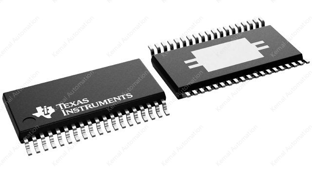
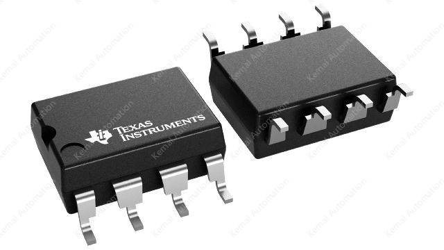
Texas Instruments Price List

Model Description Leading Price
Texas Instruments

The DRV632 is a 2-VRMS pop-free stereo line driver designed toallow the removal of the output dc-blocking capacitors for reduced component count and cost. Thedevice is ideal for single-supply electronics where size and cost are critical designparameters.

Designed using TI’s patented DirectPath™ technology, The DRV632 is capable of driving 2VRMS into a 10-kΩ load with 3.3-V supply voltage. The device hasdifferential inputs and uses external gain-setting resistors to support a gain range of ±1 V/V to±10 V/V, and gain can be configured individually for each channel. Line outputs have ±8-kV IEC ESDprotection, requiring just a simple resistor-capacitor ESD protection circuit. The DRV632 hasbuilt-in active-mute control for pop-free audio on/off control. The DRV632 has an externalundervoltage detector that mutes the output when the power supply is removed, ensuring a pop-freeshutdown.

Using the DRV632 in audio products can reduce component count considerably compared totraditional methods of generating a 2-VRMS output. The DRV632 does notrequire a power supply greater than 3.3 V to generate its 5.6-Vpp output,nor does it require a split-rail power supply. The DRV632 integrates its own charge pump togenerate a negative supply rail that provides a clean, pop-free ground-biased2-VRMS output.


The DRV632 is available in a 14-pin TSSOP.

In Stock
Subscribe

Single-channel Isolated 24-V to 60-V digital input receiver for digital input modules  

The ISO1211 and ISO1212 devices are isolated 24-V to 60-Vdigital input receivers, compliant to IEC 61131-2 Type 1, 2, and 3 characteristics. These devicesenable 9-V to 300-V DC and AC digital input modules in programmable logic controllers (PLCs),motor-control, grid infrastructure, and other industrial applications. Unlike traditionaloptocoupler solutions with discrete, imprecise current limiting circuitry, theISO121x devices provide asimple, low-power solution with an accurate current limit to enable the design of compact andhigh-density I/O modules. These devices do not require field-side power supply and are configurableas sourcing or sinking inputs.

The ISO121x devicesoperate over the supply range of 2.25 V to 5.5 V, supporting 2.5-V, 3.3-V, and 5-V controllers. A±60-V input tolerance with reverse polarity protection helps ensure the input pins are protected incase of faults with negligible reverse current. These devices support up to 4-Mbps data ratespassing a minimum pulse width of 150 ns for high-speed operation. The ISO1211 device is ideal for designsthat require channel-to-channel isolation and the ISO1212 device is ideal formultichannel space-constrained designs.

The ISO121x devicesreduce component count, simplify system design, improve performance, and reduce board temperaturescompared to traditional solutions. For details, refer to the How To Simplify Isolated 24-V PLC Digital Input ModuleDesigns TI TechNote, How To Improve Speed and Reliability of Isolated Digital Inputs in MotorDrives TI TechNote, and How to Design Isolated Comparators for ±48V, 110V and 240V DC and ACDetection TI TechNote.

In Stock
Subscribe

2.5-kVrms, isolated unidirectional clock, bidirectional I2C isolator  

The ISO1540 and ISO1541 devices are low-power, bidirectional isolators that are compatible withI2C interfaces. These devices have logic input and output buffers thatare separated by Texas Instruments Capacitive Isolation technology using a silicon dioxide(SiO2) barrier. When used with isolated power supplies, these devices blockhigh voltages, isolate grounds, and prevent noise currents from entering the local ground andinterfering with or damaging sensitive circuitry.

This isolation technology provides for function, performance, size, and power consumptionadvantages when compared to optocouplers. The ISO1540 andISO1541 devices enable a completeisolated I2C interface to be implemented within a small formfactor.

The ISO1540 has twoisolated bidirectional channels for clock and data lines while the ISO1541 has a bidirectional dataand a unidirectional clock channel. The ISO1541 is useful in applications that have a single master while theISO1540 is suitable formulti-master applications. For applications where clock stretching by the slave is possible, theISO1540 device should beused.

Isolated bidirectional communication is accomplished within these devices by offsettingthe low-level output voltage on side 1 to a value greater than the high-level input voltage on side1, thus preventing an internal logic latch that otherwise would occur with standard digitalisolators.

In Stock
Subscribe

Sitara processor: Arm Cortex-A8, video front end

(AM3517/05 is a high-performance ARM Cortex-A8 microprocessor with speeds up to 600 MHz. The device offers 3D graphics acceleration while also supporting numerous peripherals, including DDR2, CAN, EMAC, and USB OTG PHY that are well suited for industrial apllications.

The processor can support other applications, including: Single-board computers Home and industrial automation Human machine Interface

The device supports high-level operating systems (OSs), such as:

Linux®

Windows® CE

Android™

The following subsystems are part of the device:

Microprocessor unit (MPU) subsystem based on the ARM Cortex-A8 microprocessor

PowerVR SGX graphics accelerator (AM3517 device only) subsystem for 3D graphics acceleration to support display and gaming effects

Display subsystem with several features for multiple concurrent image manipulation, and a programmable interface supporting a wide variety of displays. The display subsystem also supports NTSC/PAL video out.

High-performance interconnects provide high-bandwidth data transfers for multiple initiators to the internal and external memory controllers and to on-chip peripherals. The device also offers a comprehensive clock-management scheme.

AM3517/05 devices are available in a 491-pin BGA package and a 484-pin PBGA package.

This AM3517/05 data manual presents the electrical and mechanical specifications for the AM3517/05 Sitara processor.)

In Stock
Subscribe

The Texas Instruments bq4050device, incorporating Compensated End-of-Discharge Voltage (CEDV) technology, is a highlyintegrated, accurate, 1-series to 4-series cell gas gauge and protection solution, enablingautonomous charger control and cell balancing.

The bq4050 device provides a fully integrated pack-based solution with a flashprogrammable custom reduced instruction-set CPU (RISC), safety protection, and authentication forLi-Ion and Li-Polymer battery packs.

The bq4050 gas gauge communicates via an SMBus-compatible interface and combines anultra-low power, high-speed TI bqBMP processor, high-accuracy analog measurement capabilities,integrated flash memory, an array of peripheral and communication ports, an N-CH FET drive, and aSHA-1 Authentication transform responder into a complete, high-performance battery managementsolution.

1-4 series CEDV battery fuel (gas) gauge

In Stock
Subscribe

High-side n-channel FET driver

The bq76200 device is a low-power, high-side, N-channel system. Ahigh-side protection avoids ground disconnection in the system and also allows continuouscommunication between the battery pack and host system. The device has additional P-Channel FETcontrol to allow low-current pre-charge to a deeply depleted battery, and a PACK+ voltage monitorcontrol for the host to sense the PACK+ voltage.

The independent enable inputs allow CHG and DSG FETs to be turned onand off separately, offering great implementation flexibility in battery systems.

The bq76200 device can be used with a companion analog front end (AFE)device such as the bq76920/30/40 family, a 3-series to 15-series Cell Analog Front End Monitoring,and a host microcontroller or dedicated state-of-charge (SOC) tracking gas gauge device.

In Stock
Subscribe

Low-power Sub-1 GHz wireless transceiver

CC1101 is a low-cost sub-1 GHz transceiver designed for very low-power wireless applications. The circuit is mainly intended for the ISM (Industrial, Scientific and Medical) and SRD (Short Range Device) frequency bands at 315, 433, 868, and 915 MHz, but can easily be programmed for operation at other frequencies in the 300-348 MHz, 387-464 MHz and 779-928 MHz bands.

The RF transceiver is integrated with a highly configurable baseband modem. The modem supports various modulation formats and has a configurable data rate up to 600 kbps.


CC1101 provides extensive hardware support for packet handling, data buffering, burst transmissions, clear channel assessment, link quality indication, and wake-on-radio.

The main operating parameters and the 64- byte transmit/receive FIFOs of CC1101 can be controlled via an SPI interface. In a typical system, the CC1101 will be used together with a microcontroller and a few additional passive components.


The CC1190 850-950 MHz range extender [21] can be used with CC1101 in long range applications for improved sensitivity and higher output power.

In Stock
Subscribe

Value line Sub-1 GHz wireless transmitter 

Few External Components; Fully Integrated Frequency Synthesizer

Green Package: RoHS Compliant and No Antimony or Bromine

Small Size (QLP 4x4 mm Package, 20 pins)

Suited for Systems Targeting Compliance with EN 300 220 (Europe) and FCC CFR Part 15 (US)

Support for Asynchronous and Synchronous Serial Transmit Mode for Backwards Compatibility with Existing Radio Communication Protocols

The CC115L is a cost optimized sub-1 GHz RF transmitter. The circuit is based on the popular CC1101 RF transceiver, and RF performance characteristics are identical. The CC115L value line transmitter together with the CC113L value line receiver enables a low cost RF link.

The RF transmitter is integrated with a configurable baseband modulator. The modem supports various modulation formats and has a configurable data rates from 0.6 to 600 kbps.

CC115L provides extensive hardware support for packet handling, data buffering and burst transmissions.

The main operating parameters and the 64- byte transmit FIFO of CC115L can be controlled via an SPI interface. In a typical system, the CC115L will be used together with a microcontroller and a few additional passive components.

In Stock
Subscribe

12-V, N channel NexFET™ power MOSFET, single LGA 1 mm x 0.6mm, 180 mOhm, gate ESD protection                                                                                                                      

This 140-mΩ, 12-V N-channel FemtoFET™ MOSFET technology is designed and optimized to minimize the footprint in many handheld and mobile applications. This technology is capable of replacing standard small signal MOSFETs while providing at least a 60% reduction in footprint size.

In Stock
Subscribe

30-V, N channel NexFET™ power MOSFET, single SON 2 mm x 2 mm, 32 mOhm                                     

 This 30-V, 24-mΩ, 2-mm × 2-mm SON NexFET™ power MOSFET is designed to minimize losses in power conversion applications and optimized for 5-V gate drive applications. The 2-mm × 2-mm SON offers excellent thermal performance for the size of the package.

In Stock
Subscribe

The -12-V, P channel NexFET™ power MOSFET, single LGA 0.6 mm x 0.7 mm, 116 mOhm, gate ESD protection                                                                                                             

 G66This –12-V, 97-mΩ, P-Channel FemtoFET™ MOSFET is designed and optimized to minimize the footprint in many handheld and mobile applications. This technology is capable of replacing standard small signal MOSFETs while providing a substantial reduction in footprint size.

In Stock
Subscribe

Dual-channel, 2/0, 150-Mbps digital isolator  

The ISO7220x and ISO7221x family devices are dual-channel digital isolators. To facilitate PCB layout, the channels are oriented in the same direction in the ISO7220x and in opposite directions in the ISO7221x. These devices have a logic input and output buffer separated by TI’s silicon-dioxide (SiO2) isolation barrier, providing galvanic isolation of up to 4000 VPK per VDE. Used in conjunction with isolated power supplies, these devices block high voltage and isolate grounds, as well as prevent noise currents on a data bus or other circuits from entering the local ground and interfering with or damaging sensitive circuitry.

A binary input signal is conditioned, translated to a balanced signal, then differentiated by the capacitive isolation barrier. Across the isolation barrier, a differential comparator receives the logic transition information, then sets or resets a flip-flop and the output circuit accordingly. A periodic update pulse is sent across the barrier to ensure the proper dc level of the output. If this dc-refresh pulse is not received every 4 µs, the input is assumed to be unpowered or not being actively driven, and the failsafe circuit drives the output to a logic high state.

The small capacitance and resulting time constant provide fast operation with signaling rates available from 0 Mbps (DC) to 150 Mbps (The signaling rate of a line is the number of voltage transitions that are made per second expressed in the units bps). The A-option, B-option, and C-option devices have TTL input thresholds and a noise filter at the input that prevents transient pulses from being passed to the output of the device. The M-option devices have CMOS VCC/2 input thresholds and do not have the input noise filter and the additional propagation delay.

The ISO7220x and ISO7221x family of devices require two supply voltages of 2.8 V (C-Grade), 3.3 V, 5 V, or any combination. All inputs are 5-V tolerant when supplied from a 2.8-V or 3.3-V supply and all outputs are 4-mA CMOS.

The ISO7220x and ISO7221x family of devices are characterized for operation over the ambient temperature range of –40°C to +125°C.

In Stock
Subscribe

18-channel I2C constant-current RGB LED driver

In smart homes and other applications that utilize human-machine-interaction,high-performance RGB LED drivers are required. LED animation effects such as flashing, breathing,and chasing greatly improve user experience, and minimal system noise is essential.

The LP50xx device is an 18- or 24-channel constant current sink LED driver. The LP50xxdevice includes integrated color mixing and brightness control, and pre-configuration simplifiesthe software coding process. Integrated 12-bit, 29 kHz PWM generators for each channel enablesmooth, vivid color for LEDs, and eliminate audible noise.

The LP50xx device controls each LED output with a 12-bit PWM resolution at 29-kHzswitching frequency, which helps achieve a smooth dimming effect and eliminates audible noise. Theindependent color mixing and intensity control registers make the software coding straightforward.When targeting a fade-in, fade-out type breathing effect, the global R, G, B bank control reducesthe microcontroller loading significantly. The LP50xx device also implements a PWM phase-shiftingfunction to help reduce the input power budget when LEDs turn on simultaneously.

The LP50xx device implements an automatic power-saving mode to achieve ultralow quiescentcurrent. When channels are all off for 30 ms, the device total power consumption is down to 10 µA,which makes the LP50xx device a potential choice for battery-powered end equipment.   

In Stock
Subscribe

24-bit, 2-kSPS, 4-ch, low-power, small-size delta-sigma ADC w/ PGA, VREF, 2x IDACs & SPI interfaceData converters

The ADS1220 is a precision, 24-bit, analog-to-digital converter (ADC) that offers many integrated features to reduce system cost and component count in applications measuring small sensor signals. The device features two differential or four single-ended inputs through a flexible input multiplexer (MUX), a low-noise, programmable gain amplifier (PGA), two programmable excitation current sources, a voltage reference, an oscillator, a low-side switch, and a precision temperature sensor.

The device can perform conversions at data rates up to 2000 samples-per-second (SPS) with single-cycle settling. At 20 SPS, the digital filter offers simultaneous 50-Hz and 60-Hz rejection for noisy industrial applications. The internal PGA offers gains up to 128 V/V. This PGA makes the ADS1220 ideally-suited for applications measuring small sensor signals, such as resistance temperature detectors (RTDs), thermocouples, thermistors, and resistive bridge sensors. The device supports measurements of pseudo- or fully-differential signals when using the PGA. Alternatively, the device can be configured to bypass the internal PGA while still providing high input impedance and gains up to 4 V/V, allowing for single-ended measurements.

Power consumption is as low as 120 µA when operating in duty-cycle mode with the PGA disabled. The ADS1220 is offered in a leadless VQFN-16 or a TSSOP-16 package and is specified over a temperature range of –40°C to +125°C.

In Stock
Subscribe

Standalone 1-cell 1-A linear battery charger with 4.2-V VBAT and Temperature Sensing   

The BQ2404x series of devices are highly integrated Li-Ion and Li-Pol linear chargers devices targeted at space-limited portable applications. The devices operate from either a USB port or AC adapter. The high input voltage range with input overvoltage protection supports low-cost unregulated adapters.

The BQ2404x has a single power output that charges the battery. A system load can be placed in parallel with the battery as long as the average system load does not keep the battery from charging fully during the 10 hour safety timer.

The battery is charged in three phases: conditioning, constant current and constant voltage. In all charge phases, an internal control loop monitors the IC junction temperature and reduces the charge current if an internal temperature threshold is exceeded.

The charger power stage and charge current sense functions are fully integrated. The charger function has high accuracy current and voltage regulation loops, charge status display, and charge termination. The pre-charge current and termination current threshold are programmed through an external resistor on the BQ24040 and BQ24045. The fast charge current value is also programmable through an external resistor.


In Stock
Subscribe

The BQ2407x series of devices are integrated Li-Ion linear chargers and system power path management devices targeted at space-limited portable applications. The devices operate from either a USB port or an AC adapter and support charge currents up to 1.5 A. The input voltage range with input overvoltage protection supports unregulated adapters. The USB input current limit accuracy and start up sequence allow the BQ2407x to meet USB-IF inrush current specifications. Additionally, the input dynamic power management (VIN-DPM) prevents the charger from crashing incorrectly configured USB sources.

The BQ2407x features dynamic power path management (DPPM) that powers the system while simultaneously and independently charging the battery. The DPPM circuit reduces the charge current when the input current limit causes the system output to fall to the DPPM threshold; thus, supplying the system load at all times while monitoring the charge current separately. This feature reduces the number of charge and discharge cycles on the battery, allows for proper charge termination and enables the system to run with a defective or absent battery pack.

Additionally, the regulated system input enables instant system turn-on when plugged in even with a totally discharged battery. The power path management architecture also lets the battery supplement the system current requirements when the adapter cannot deliver the peak system currents, thus enabling the use of a smaller adapter.

The battery is charged in three phases: conditioning, constant current, and constant voltage. In all charge phases, an internal control loop monitors the IC junction temperature and reduces the charge current if the internal temperature threshold is exceeded. The charger power stage and charge current sense functions are fully integrated. The charger function has high accuracy current and voltage regulation loops, charge status display, and charge termination. The input current limit and charge current are programmable using external resistors.

Standalone 1-cell 1.5-A linear battery charger, Power Path, 4.2-V VBAT and 4.4-V

In Stock
Subscribe

The BQ2407x series of devices are integrated Li-Ion linear chargers and system power path management devices targeted at space-limited portable applications. The devices operate from either a USB port or an AC adapter and support charge currents up to 1.5 A. The input voltage range with input overvoltage protection supports unregulated adapters. The USB input current limit accuracy and start up sequence allow the BQ2407x to meet USB-IF inrush current specifications. Additionally, the input dynamic power management (VIN-DPM) prevents the charger from crashing incorrectly configured USB sources.

The BQ2407x features dynamic power path management (DPPM) that powers the system while simultaneously and independently charging the battery. The DPPM circuit reduces the charge current when the input current limit causes the system output to fall to the DPPM threshold; thus, supplying the system load at all times while monitoring the charge current separately. This feature reduces the number of charge and discharge cycles on the battery, allows for proper charge termination and enables the system to run with a defective or absent battery pack.

Additionally, the regulated system input enables instant system turn-on when plugged in even with a totally discharged battery. The power path management architecture also lets the battery supplement the system current requirements when the adapter cannot deliver the peak system currents, thus enabling the use of a smaller adapter.

The battery is charged in three phases: conditioning, constant current, and constant voltage. In all charge phases, an internal control loop monitors the IC junction temperature and reduces the charge current if the internal temperature threshold is exceeded. The charger power stage and charge current sense functions are fully integrated. The charger function has high accuracy current and voltage regulation loops, charge status display, and charge termination. The input current limit and charge current are programmable using external resistors.

Standalone 1-cell 1.5-A linear battery charger, Power Path, 4.2-V VBAT and 4.4-V 

In Stock
Subscribe

The bq24259 is a highly-integrated switch-mode battery charge management and system power path management device for 1 cell Li-Ion and Li-polymer battery in a wide range of smart phone and tablet applications. Its low impedance power path optimizes switch-mode operation efficiency, reduces battery charging time and extends battery life during discharging phase. The I2C serial interface with charging and system settings makes the device a truly flexible solution.

The device supports 3.9 V – 6.2 V USB input sources, including standard USB host port and USB charging port with 6.4 V overvoltage protection. The device supports USB 2.0 and USB 3.0 power specifications with input current and voltage regulation. To set the default input current limit, the bq24259 takes the result from the detection circuit in the system, such as USB PHY device. The device also supports USB On-the-Go operation by providing fast startup and supplying adjustable voltage 4.55 V – 5.5 V (default 5 V) on the VBUS with an accurate current limit up to 1.5 A.

The power path management regulates the system slightly above battery voltage but does not drop below 3.5 V minimum system voltage (programmable). With this feature, the system keeps operating even when the battery is completely depleted or removed. When the input source current or voltage limit is reached, the power path management automatically reduces the charge current to zero and then starts discharges the battery until the system power requirement is met. This supplement mode operation keeps the input source from getting overloaded.

The device initiates and completes a charging cycle when host control is not available. It automatically charges the battery in three phases: pre-conditioning, constant current and constant voltage. In the end, the charger automatically terminates when the charge current is below a preset limit in the constant voltage phase. Later on, when the battery voltage falls below the recharge threshold, the charger will automatically start another charging cycle.

The charge device provides various safety features for battery charging and system operation, including negative thermistor monitoring, charging safety timer and over-voltage/over-current protections. The thermal regulation reduces charge current when the junction temperature exceeds 120°C (programmable).

The STAT output reports the charging status and any fault conditions. The INT immediately notifies host when fault occurs.

The bq24259 is available in a 24-pin, 4 × 4 mm2 thin VQFN package.

I2C controlled 2A single cell USB NVDC-1 charger with adjustable voltageUSB OTG

In Stock
Subscribe

I2C controlled 1-cell, 3-A battery charger with USB NVDC-1, adj. voltage, and USB OTG with D+/D-

The bq24296/bq24297 are highly-integrated switch-mode battery charge management and system power path management devices for 1 cell Li-Ion and Li-polymer batteries in a wide range of smart phone and tablet applications.

Its low impedance power path optimizes switch-mode operation efficiency, reduces battery charge time and extends battery life during discharging phase. The I2C serial interface with charging and system settings makes the device a truly flexible solution.

The device supports 3.9-V to 6.2-V USB input sources, including standard USB host port and USB charging port with 6.4-V over-voltage protection. The device is compliant with USB 2.0 and USB 3.0 power specifications with input current and voltage regulation. To set the default input current limit, the bq24296 takes the result from the detection circuit in the system, such as USB PHY device and the bq24297 detects the input source through D+/D– detection following the USB battery charging spec 1.2. In addition, the bq24297 detects non-standard 2-A/1-A adapters. The device also supports USB On-the-Go operation by providing fast startup and supplying adjustable voltage 4.55-V to 5.5-V (default 5 V) on the VBUS with an accurate current limit up to 1.5 A.

The power path management regulates the system slightly above battery voltage but does not drop below 3.5-V minimum system voltage (programmable). With this feature, the system keeps operating even when the battery is completely depleted or removed. When the input source current or voltage limit is reached, the power path management automatically reduces the charge current to zero and then starts discharges the battery until the system power requirement is met. This supplement mode operation keeps the input source from getting overloaded.

The device initiates and completes a charging cycle when host control is not available. It automatically charges the battery in three phases: pre-conditioning, constant current, and constant voltage. In the end, the charger automatically terminates when the charge current is below a preset limit in the constant voltage phase. Later on, when the battery voltage falls below the recharge threshold, the charger automatically starts another charging cycle.

The charge device provides various safety features for battery charging and system operation, including negative thermistor monitoring, charging safety timer, and over-voltage/over-current protections. The thermal regulation reduces charge current when the junction temperature exceeds 120°C (programmable).

The STAT output reports the charging status and any fault conditions. The INT immediately notifies the host when a fault occurs.

The bq24296 and bq24297 are available in a 24-pin, 4.00 × 4.00 mm2 thin VQFN package.

In Stock
Subscribe

The BQ2970 battery cell protection device provides an accurate monitor and trigger threshold for overcurrent protection during high discharge/charge current operation or battery overcharge conditions.

The BQ2970 device provides the protection functions for Li-ion/Li-polymer cells, and monitors across the external power FETs for protection due to high charge or discharge currents. In addition, there is overcharge and depleted battery monitoring and protection. These features are implemented with low current consumption in NORMAL mode operation.

Li-Ion/Li Polymer Advanced Single-Cell Battery Protector IC Family        

In Stock
Subscribe

The BQ2970 battery cell protection device provides an accurate monitor and trigger threshold for overcurrent protection during high discharge/charge current operation or battery overcharge conditions.

The BQ2970 device provides the protection functions for Li-ion/Li-polymer cells, and monitors across the external power FETs for protection due to high charge or discharge currents. In addition, there is overcharge and depleted battery monitoring and protection. These features are implemented with low current consumption in NORMAL mode operation.

Li-Ion/Li Polymer Advanced Single-Cell Battery Protector IC Family         

In Stock
Subscribe

Analog front end for 3 to 6 series lithium-ion cells

BQ76925 host-controlled analog front end (AFE) is part of a complete pack monitoring,balancing, and protection system for 3-, 4-, 5-, or 6-series cell li-ion and li-polymer batteries.The BQ76925 device allows a host controller to monitor individual cell voltages, pack current andtemperature easily. The Host may use this information to determine unsafe or faulty operatingconditions such as overvoltage, undervoltage, overtemperature, overcurrent, cell imbalance, stateof charge, and state of health conditions.

Cell input voltages are level-shifted, multiplexed, scaled, and output for measurement bya host ADC. A dedicated pin provides a low-drift calibrated reference voltage to enable accuratemeasurements.

The voltage across an external-sense resistor is amplified and output to a host ADC forboth charge and discharge current measurements. Two gain settings enable operation with a varietyof sense resistor values over a wide range of pack currents.

To enable temperature measurements by the host, the AFE provides a separate output pinfor biasing an external thermistor network. This output can be switched on and off under hostcontrol to minimize power consumption.

The BQ76925 device includes a comparator with a dynamically selectable threshold formonitoring current. The comparator result is driven through an open-drain output to alert the hostwhen the threshold is exceeded. This feature can be used to wake up the host on connection of theload, or to alert the host to a potential fault condition.

The BQ76925 device integrates cell balancing FETs that are fully controlled by the host.The balancing current is set by external resistors up to a maximum value of 50 mA. These same FETsmay be utilized in conjunction with cell voltage measurements to detect an open wire on a cellsense-line.

The host communicates with the AFE through an I2C interface. Apacket CRC may optionally be used to ensure robust operation. The device may be put into alow-current sleep mode through the I2C interface and awakened by pullingup the ALERT pin.)

In Stock
Subscribe

3-s to 16-s high-accuracy battery monitor and protector for Li-ion, Li-polymer and LiFePO4

The Texas Instruments BQ76952 device is a highly integrated, high-accuracy battery monitor and protector for 3-series to 16-series Li-ion, Li-polymer, and LiFePO4 battery packs. The device includes a high-accuracy monitoring system, a highly configurable protection subsystem, and support for autonomous or host controlled cell balancing. Integration includes high-side charge-pump NFET drivers, dual programmable LDOs for external system use, and a host communication peripheral supporting 400-kHz I2C, SPI, and HDQ one-wire standards. The BQ76952 device is available in a 48-pin TQFP package.

In Stock
Subscribe

6-ch, 3-V to 18-V inverters   

The CD4069UB device consist of six CMOS inverter circuits. These devices are intendedfor all general-purpose inverter applications where the medium-power TTL-drive andlogic-level-conversion capabilities of circuits such as the CD4009 and CD4049 hex inverter andbuffers are not required.


In Stock
Subscribe

12-V, N channel NexFET™ power MOSFET, single LGA 1 mm x 0.6mm, 44 mOhm, gate ESD protection                                                                                                                             Power management

This 37 mΩ, 12 V N-channel FemtoFET™ MOSFET technology is designed and optimized to minimize the footprint in many handheld and mobile applications. This technology is capable of replacing standard small signal MOSFETs while providing at least a 60% reduction in footprint size.


In Stock
Subscribe

Synchronous Buck NexFET Power Stage, CSD95379Q3M                                               

 The CSD95379Q3M NexFET™ power stage is a highly optimized design for use in high-power, high-density synchronous buck converters. This product integrates the driver IC and NexFET technology to complete the power stage switching function. The driver IC has a built-in selectable diode emulation function that enables DCM operation to improve light load efficiency. In addition, the driver IC supports ULQ mode that enables Connected Standby for Windows® 8. With the PWM input in tri-state, quiescent current is reduced to 130 µA, with immediate response. When SKIP# is held at tri-state, the current is reduced to 8 µA (typically 20 µs is required to resume switching). This combination produces high-current, high-efficiency, and high-speed switching capability in a small 3.3-mm × 3.3-mm outline package. In addition, the PCB footprint has been optimized to help reduce design time and simplify the completion of the overall system design.

In Stock
Subscribe

52-V, bipolar stepper motor gate driver with 1/256 microstepping & stall detect  

The DRV8711 device is a stepper motor controller that uses external N-channel MOSFETs todrive a bipolar stepper motor or two brushed DC motors. A microstepping indexer is integrated,which is capable of step modes from full step to 1/256-step.

An ultra-smooth motion profile can be achieved using adaptive blanking time and variouscurrent decay modes, including an auto-mixed decay mode. Motor stall is reported with an optionalback-EMF output.

A simple step/direction or PWM interface allows easy interfacing to controller circuits.A SPI serial interface is used to program the device operation. Output current (torque), step mode,decay mode, and stall detection functions are all programmable through a SPI serialinterface.

Internal shutdown functions are provided for overcurrent protection, short-circuitprotection, undervoltage lockout, and overtemperature. Fault conditions are indicated through aFAULTn pin, and each fault condition is reported through a dedicated bit through SPI.

The DRV8711 is packaged in a PowerPAD™38-pin HTSSOP package with thermal pad (Eco-friendly: RoHS and no Sb/Br).

In Stock
Subscribe

Isolated 5-V CAN transceiver    

The ISO1050 is a galvanically isolated CAN transceiver that meets the specifications of the ISO11898-2 standard. The device has the logic input and output buffers separated by a silicon oxide (SiO2) insulation barrier that provides galvanic isolation of up to 5000 VRMS for ISO1050DW and 2500 VRMS for ISO1050DUB. Used in conjunction with isolated power supplies, the device prevents noise currents on a data bus or other circuits from entering the local ground and interfering with or damaging sensitive circuitry.

As a CAN transceiver, the device provides differential transmit capability to the bus and differential receive capability to a CAN controller at signaling rates up to 1 megabit per second (Mbps). The device is designed for operation in especially harsh environments, and it features cross-wire, overvoltage and loss of ground protection from –27 V to 40 V and overtemperature shutdown, as well as –12-V to 12-V common-mode range.

The ISO1050 is characterized for operation over the ambient temperature range of –55°C to 105°C._

In Stock
Subscribe

  100-mA, 30-V, low-dropout voltage regulator with power good & enable

LP2950 and LP2951 devices are bipolar, low-dropout voltage regulators that can accommodate a wide input supply-voltage range of up to 30 V. The easy-to-use, 3-pin LP2950 is available in fixed-output voltages of 5 V, 3.3 V, and 3 V. However, the 8-pin LP2951 is able to output either a fixed or adjustable output from the same device. By tying the OUTPUT and SENSE pins together, and the FEEDBACK and VTAP pins together, the LP2951 outputs a fixed 5 V, 3.3 V, or 3 V (depending on the version). Alternatively, by leaving the SENSE and VTAP pins open and connecting FEEDBACK to an external resistor divider, the output can be set to any value between 1.235 V to 30 V.)

In Stock
Subscribe
Unsubscribe

Discount Code

Subscribe
Please check the item(s) you are interested in. (required)

Enter email to obtain information:

Verification code:

verify-code
USE : 0.23264384269714